Wednesday, May 30, 2012

Complex Numbers with FreeMat

Introduction


One of the usefulness of FreeMat is to be able to calculate complex operation easily. Complex operation is really important for engineers since all the AC signal involving inductor and capacitor will have a complex impedance and when doing more complex circuit, complex analysis can become tedious. The FreeMat program definitely helps in complex analysis.


Operations with complex number:
Excercise 1


Function to convert from rectangular to polar
Exercise 1&2

Assignment

Op-Amps as an Integrator


Introduction

            One of the uses of the op-amps in this lab is to be an integrator of an AC signal. There are several types of signals that could be generated through the function generator. In this lab, we will try to integrate the square, triangle, sine and sawtooth signals and observe the output signal after it is being integrated by the op-amps. What it means by integrated is the mathematical calculation called integral will be done to the signals through the op-amps

Experimental

Before setting up the circuit, some predictions are made concerning the shape of the output as shown below:


The op amps acts as an integrator since:
Vin / Rin = iC
dq/dt = C dV/dt = iC

Now in order to have V,
V = 1/(RinC) * Vin(t)dt

The schematic shown in the picture above did not have an expected result so in order to compensate for it, new values for the components are used as shown in the table below:

Component
Nominal Value
Actual Value
C
47µF
46.6 ± .01µF
Rin
100kΩ
102.7 ± 0.1 kΩ
Rp
100MΩ
9.94 ± .1 MΩ

The setup of the circuit is as follow:


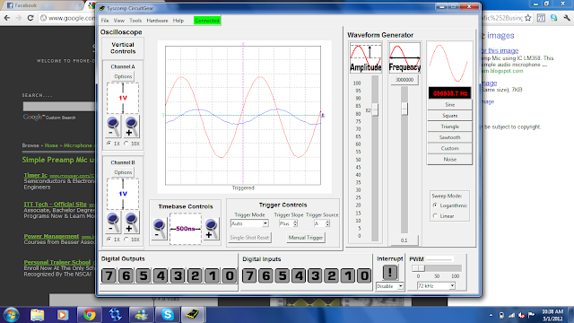
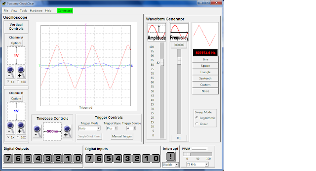
The probe is connected so that red represent the input while blue represent the output. The result of the reading is as follow:
Sawtooth signal

sine wave signal


Square wave signal
Triangle signal


Questions:

  1. The 10MΩ parallel resistor is needed so that the capacitor does not saturate the low frequency signal as the resistor will take over and act as a regular op amps instead. A huge resistor is used so that the effect will be apparent when the impedance in the capacitor increased greatly.
  2. When integrating a constant voltage, in this case a DV voltage, it will charge the capacitor and it will make the capacitor act as an open circuit which also make all the current goes to the resistor leading to not an integrator but a regular gain op-amps.
  3. When the parallel resistor is taken, the capacitor will only integrate the frequency setting it designed to do and will saturate the output when its dealing with low frequency.

Capacitor Charging and Discharging

 Introduction
       
          Capacitor are components that enable the storage of electrical energy via electric field. In this lab, we will plot the graph of the charging and the discharging of capacitors. In this lab we will design, build and test a charge/discharge system that utilizes a 10V DC power supply, employs a charging interval of about 20 seconds with a resulting energy of 2.5 mJ in 2 seconds.

Experimental

The first task that is done is to do the calculation to obtain the required Capacitance
E = 0.5 Cq^2
C = 2E / q^2 = 61.7 µF

Since we don't have capacitor with such values, 66µF will be used.

Assuming an ideal capacitance, the value of the charging resistance can be calculated

5* time constant = 20s
time constant = 4


RC = 4
R = 60.6 k_ohm


From the value above, we can calculate peak current and peak power


I = 9V/606kohms = 0.149mA
P = 0.149 (9) = 1.341mW


We then calculate the discharge resistance the same way we calculate the charging resistance
R = 6.06kohms


Again the discharge peak current and peak power is calculated


I = 9/6.06 = 1.49mA
P= 1.49(9) = 13.4mW


Once everything is calculated, the circuit was built as follow:

The capacitor put in parallel

2 variable boxes one for charging and the other for discharging

graph of charging and discharging


By looking at the graph above, when its charging, the V final is 8.45V

The resistor leakage is calculated to be 1.03Mohms

Further it discharge in 2.5 seconds

Questions


Charging:
Vth = [Rl/(R+Rl)] Vs = 8.50V

Rth = (Rl*R)/(Rl+R) = 57.2kohms

discharging:

Vth = 8.50V

Rth = 6.025kohms


Vc(τ) = .6321*(8.45V)
Vc(τ) = 5.34V
 t = 21.05s
τcharge = 21.05s
Rth = τcharge/C
Rth = 57.8kΩ

Impedance and AC Analysis 1

Introduction 
             Inductor is one of circuit element that we will explore in this lab today. A real inductor model must include a series resistance to account for the many resistance of the many turns of wire. In this lab, we will try to characterize a real inductor. We will also observe what happen to the AC signal if we have an RLC circuit

Experimental
The first step that is done is to measure the resistor value of the inductor which appears to be 9.5 ohms

Next, the external resistance was measured and it appear to be 69.1 ohms


The FG was then energized with a sinusoid output of 5000Hz frequency.

The voltage of this setting turns out to be 2.01V

Once the components have been measured, the following circuit was built
Circuit diagram for the RC circuit

The o-scope graph of the RC circuit

Data for the RC circuit:

Vin,rms = 0.884V
Iin,rms = 5.4 mA

The voltage reading differ from the FG display value probably due to the FG's internal resistance.

The impedance can also then be calculated as follow:

Z = V/I = 164ohms

Once impedance is solved, the value of the unknown inductor can be solved:
Z = Rr +Rl +jwL
L = (Z -Rr -Rl) / jw
w = angular frequency = 2*pi*f = 31416rad/s
L = 0.00272H

Part 2- RLC Circuit

First we have to calculate the value of the capacitor required to cancel out the inductance from before. The calculation is as follow:

jwL = -1/jwC
jwL = j/wC

canceling j gives the expression:
wL= 1/wC
C = 1/w^2*L
C= 23.3 nF

Once the capacitance is calculated, the following circuit is built:

RLC circuit
o-scope projection of the RLC circuit at 20kHz
 
Data:
Vpk-pk,ch1 = 2.66V
Vpk-pk,ch2 = 6.04V
Time difference = 17.57µs

From the data phase angle can be calculated


The data for different frequency is also tabulated below:

Frequency
Vin
Iin
|Zin|
5kHz
1.95V
0.1mA
19.5kΩ
10kHz
1.84V
0.1mA
18.4kΩ
20kHz
0.92V
0.4mA
2.3kΩ
30kHz
1.31V
0
50kHz
1.84V
0

Questions


  1. The input current is largest in 20kHz because we set the capacitive and inductive impedance to be equal in this frequency, which makes the imaginary part of the circuit impedance equal to zero
  2. ZL = RL + jωL
      Zin = (Rext + RL) + jωL
         V = 6.04V
          VL = (ZL/Zin)*V = 4.22 at 86.2°
            Vpp,ch2/√2 = 4.27V
          1. when we decrease the frequency, the circuit will look more capacitive since decreasing frequency means increasing capacitive impedance.
          2. When we increase frequency, the circuit will look more inductive since increasing frequency means increasing the inductive impedance


          Sunday, May 27, 2012

          AC Signals

          Introduction 
                      In this lab, we will focus on measuring the phase difference between AC sinusoidal signals at the same frequency. In this lab, we will use an integrated function generator and oscilloscope. In this lab, we will learn how to read the oscilloscope, calculate the phase shift and also the time difference to show which signal lead or lag which.

          Experimental

          The function generator and the o-scope used is as follow:
          when the probe is connected to the output, and when 1kHz is used, the data is as follow:

          Vrms from o-scope = 2.489 V
          Vrms from DMM = 2.13V

          The complex impedance of the 100 nF capacitor was then calculated:
          Z= 1/jwC = -1591j

          After the impedance is calculated, this circuit was built:

          The graph from the o-scope obtained is as follow:

          The data taken is as follow:
          Vpk-pk = 5.64V
          Vrms from DMM = 1.70V

          The value of the voltage doesn't reconcile.

          The time difference measured is 81µs

          The phase angle between the 2 signals are 39.2 degree which also means that R leads C

          Once all the data has been taken the frequency is increased to 10kHz.
          The new impedance was calculated to be 159.2 ohm

          again the graph is captured as shown below

          The data is taken and listed below:
          Vpk-pk = 1.06V
          Vrms = 0.06V

          The value between DMM and o-scope is again off by 0.3

          The time difference between peak is 24.32µs

          the phase angle between two signals is 87.6 degree

          For the next part, the frequency is turned back to 1 kHz and the resistance box is set to 10kohms
          The data taken is shown below:

          Vpk-pk = 1.21V
          Vrms = 0.32V

          The value again does not reconcile.

          The time difference between peak is 232.43µs with phase angle of 83.7 degree

           The next part is to toggle the resistor box so that the voltage is 4V peak to peak.

          R = 1.8kohms
          Vrms = 1.23V

          time difference for this is 135.14µs with phase angle of 48.65 degree.

          Conclusion and Questions

                     When the FG is on high frequency, the amplitude gets smaller while on low frequency, the amplitude gets higher. This is similar a low pass filter where it will pass all the low frequency and as it gets to higher frequency, the signal gets smaller. The resistor leads as frequency gets higher and at high frequency, the phase angle tend to be at 90 degree.

          Saturday, May 26, 2012

          Op-Amps Application

          Introduction
                    Op-amps are often used for scaling and level-shifting application. Scaling is simply process of multiplying signal voltage, in this case by factor of the gain. level shifting is the process of adding constant to a signal.in this lab, we will use a thermal sensor that produces temperature reading in Celsius and the goal of this lab is to change the reading into Fahrenheit scale.

          Experimental

          The circuit that was built is as follow:


          The value was obtained through the equation Vf = (1 +R2/R1)Vc - R2/R1 Vref

          Vref is dropping the 9V through a potentiometer and crank it accordingly.

          The actual circuit built was shown below

          Conclusion 
                    The experiment was a success as we test the input from the temperature sensor and the output of the op-amps. One of the value tested is room temperature at 23 degree celcius read in 23mV. This gets amplified and the reading in our DMM become 73.4 which is approximately the temperature in fahrenheit.

          Operational Amplifiers I

          Introduction
                     In this lab, a new circuit element called an operational amplifiers is used. As the name suggest, operational amplifier amplifies the signal of the input and it could invert or not-invert the signals. In this lab, we will use LM741 op-amps. The problems that we will tackle in this lab is a sensor whose output range is 0 to +1V has to be conditioned so that the output range between 0 and -10V. This means that the input signal should have a gain of -10. Some constraints that this lab has is that it must draw no more than 1 mA current from sensor and op-amps power supply should supply no more than 30 mW of power each.

          Experimental

          The first step of this experiment is to do some calculation

          Since the gain have to be 10, and  the max input is 1 V with 1 mA, the resistor can be calculated using

          Ri = V/ I = 1/0.001 = 1k_ohm

          The gain of the inverting op-amps is dictated by the equation: gain = Rf/Ri

          From this we know that Rf = 10Ri to get the gain of 10 and so

          Rf = 10k_ohm

          In this experiment, because of some difficulties in doing the gain of 10, we change into the gain of 5 which means the new Rf = 5k_ohm.

          The circuit diagram for this lab is as follow:


          In order to have the 0 to 1 V as the problems specified, voltage division is necessary and since, in this case, 7.5 V is used with power rating 1/8 W,

          Rx = 8* V^2 = 450 ohm

          By using voltage division method, Ry can be found to be 69.2 ohm

          Since the Rx and Ry is already solved, thevenin resistance is calculated

          R_th = Rx||Ry = 60 ohm

          The value of the thevenin resistant in this case is about 20 times smaller than the Ri

          Before building any circuit, some components were measured:

          Component
          Nominal Value
          Measured Value
          Power/Current Rating
          Ri
          1k Ω
          .984k ±.01kΩ
          .25W
          Rf
          5.2k Ω
          5.14k ±.01kΩ
          .25W
          Rx
          450 Ω
          450 ±1Ω
          1W
          Ry
          60 Ω
          57.3 ±1Ω
          1W
          V1
          7.5V
          7.54 ±.01V
          2A
          V2
          7.5V
          7.66 ±.01V
          2A 
           
          After the components have been measured,the circuit was then built as follow


           Measurements of the circuits was then taken and tabulated below:

          Vin
          Vout
          GAIN
          VRi
          IRi
          VRf
          0.0V
          0V
          0
          0V
          0mA
          0V
          .26V
          -1.42 ±.01V
          -5.46
          .26 ±.01V
          .26mA
          -1.42 ±.01V
          .51V
          -2.74 ±.01V
          -5.37
          .51 ±.01V
          .52mA
          -2.74 ±.01V
          .76V
          -3.96 ±.01V
          -5.21
          .74 ±.01V
          .75mA
          -3.96 ±.01V
          .99V
          -5±.01V
          -5.05
          .98 ±.01V
          .996mA
          -5.18 ±.01V

          Questions and Conclusions

          As measured before, I1 = 1.01mA and I2=0.8mA
          P_1 = I1*V1 = 1.01mA*7.54V = 7.62mW
          P_2 = I1*V1 = 0.8mA*7.54V = 0.61mW

          By using the op-amps as a node, need top show that I_Ri = I_Rf
          I_Ri = 0.99V / 0.984k_ohm = 1.01mA
          I_Rf = 5.18V / 5.2 k_ohm = 0.996mA
          I_Ri = I_Rf ~ 1.01mA

          We do satisfy the constraints to supply no more than 30 mW. If we want to obtain the same gain but reduce the power, we should increase the value of the resistor while keeping the ratio  between the Ri and Rf to be equal to the gain.